PROJECTS

Energy transport and conversion
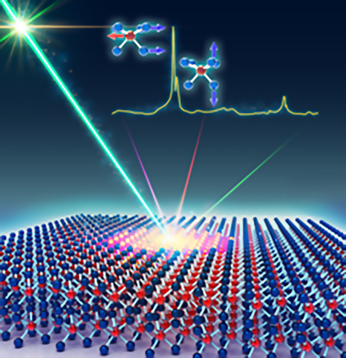
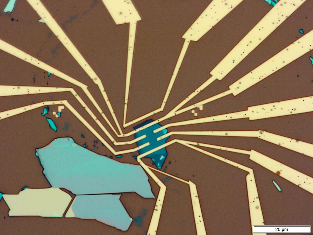
Thermal transport, thermoelectric properties continue to be of central importance in energy field. The refined opto-thermal Raman technique improved by Zhang Group leads to the first measurements of the thermal conductivity of 1- and 2-layer MoS2 and MoSe2 and the thermal properties of hBN encapsulated 2D devices, and contributes to the nanoscale phonon engineering and phononics field. Extending our existing technique in measuring thermal properties of 2D materials, we invented a dual laser at same side (DLSS) opto-thermal Raman system and incorporated a room-temperature magnetic field. With our refined opto-thermal Raman characterization and novel nanofabrication techniques, we are able to explore the thermal transport / thermoelectric properties in quantum engineered materials platforms. 2D materials to be investigated include conductors (graphene), insulators (hBN and layered organics), semiconductors (metal sulfides). topological insulators (Bismuth selenide), and ferromagnets (Chromium iodide).
Manufacturing based on low dimensional materials and heterostructures, and related flexible devices
2D atomic layer heterostructures in forms of nanoribbons as well as stacked configurations possess new emergent physical phenomena, allowing for potential new devices/circuits applications. Zhang Group is using van der Waals transfer technique, chemical doping, along with other novel manufacturing methods to build low dimensional heterostructures, flexible electronic, and origami devices. Research interest to various van der Waals material platforms include transition metal chacogenides, graphene, h-BN, etc. This study directly contributes to the fields of fluid filtration and radiation shielding.


Sensing applications of low dimensional materials (biosensor, food safety sensor, etc.)
Because of low dimensional materials’ excellent properties such as high conductance, high mobility, and chemical inertness, continuous progress has been carried out on carbon nanotube and graphene sensors for medical diagnosis, food safety, etc. For example, in one of our sensing applications, individual carbon nanotube field effect transistors are lithographically “cut” and rejoined with single molecules in the gap, to yield circuits that can be used to study the basic electrical transport properties of single molecules, and can form the basis of multiple types of sensors. The low dimensional materials’ devices are also used for growth factor detection and wearable medical diagnosis.
Investigation of low dimensional materials by deep learning algorithms
In this project, we design and use two Convolutional Neural Network (CNN) models on graphene research.

